成都一老人珍藏20年乾隆玉是块玻璃
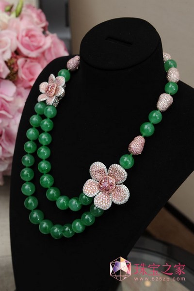
 9月28日,珠宝鉴定师向胡庆介绍玉石的真假辨识
 专家
这不是什么宝玉,只不过是一块玻璃而已
检验师
太明显了,是注胶染色的翡翠,可能只值几十元钱
当事人
心结总算是了啦,玉这个东西,自己喜欢就好
年近70岁的成都老人胡庆(化名),20年前花3万元买了一块“乾隆玉”,这些钱在当时足够买一套房子.2007年,他曾去河南参加过鉴宝活动.经过鉴定,这块“乾隆玉”实际上是一块被注胶染色的假玉,可能仅值几十元钱.
这么多年来,胡庆都不相信玉坠是假的.昨日下午,他小心翼翼地用纸包起了自己的玉坠,来到草塘东路的一家珠宝店进行鉴定.
纠结20年 乾隆玉到底是真是假?
1990年,50岁的胡庆喜欢上了收集玉石,这一天,他在送仙桥附近一家古玩店看上一个“福禄寿”玉坠.玉坠长约5厘米,边缘打磨和制作工艺较为粗犷,很像是乾隆年间的玉器.
在老板的推荐下,胡庆将妻子和自己的存款凑在一起,花3万元买下这块玉.在把玩过程中,胡庆买了不少关于玉石鉴定的书籍看,并咨询了不少行家,有人说这块玉只是一块玻璃,也有人说这块玉价值连城.此后,玉的真假便成了胡庆的心结.
首次鉴定 专家说就是一块玻璃
2007年,胡庆乘车来到郑州,带着自己的玉坠参加了一个鉴宝节目.专家拿起这块“乾隆玉”看了一下,花了不到1分钟就得出结论.
“这不是什么宝玉,只不过是一块玻璃而已.”专家的这句话让胡庆的心都凉了,在回家的路上,他几近崩溃,将所有的注意力都集中在玉上,把衣服和帽子都弄丢了.
他一度想把玉从火车的窗子上扔出去,但又觉得不甘心,毕竟玉跟了自己这么久.于是,他准备再次鉴定,期待专家的说法能够改变,说它是一块真玉.
再次鉴定 检验师说或值几十元
昨日下午,胡庆小心地包好“乾隆玉”,又拿上一条15年前花6000多元买的玉质佛珠,来到草堂北路一家珠宝店鉴定.
检验师拿起“乾隆玉”在阳光下看了一下,脱口而出,“太明显了,是注胶染色的翡翠,可能只值几十元钱.”看到胡庆有些不太相信,检验师又在灯光和显微镜下再次对玉进行了观察,同样得出了假玉的结论.
“您再给我看看这个.”感到有些失望的胡庆,又把佛珠交给检验师.“这个是染色的马来玉,质地还不如那个‘乾隆玉’.”检验师的一席话,让胡庆第二次受到打击.
不过,他怔了两秒后,还是将两块玉小心地包好,笑着说:“心结总算是了啦,玉这个东西,自己喜欢就好.”这次检验后,胡庆没有像在郑州时那样郁闷,在和检验师道别后,他默默地离开现场.
温馨提示
在电筒下识别假玉
珠宝鉴定师说,消费者可以用一种简单的方法鉴定假玉.将染色翡翠置于电筒下,会发现翡翠被染色后,玉的裂纹处颜色最深,绿色沿着裂纹充填在裂纹附近的晶粒间隙中,呈丝网状分布.而天然翡翠的裂纹和孔隙都是没有颜色的,这种方法可以对大部分“地摊货”和普通染色玉进行鉴别.
华西都市报记者崔燃实习生杨雪摄影吴小川
来源:新浪收藏
TAG:成都一老人珍藏20年乾隆玉是块玻璃 翡翠 翡翠手镯 中国翡翠网 翡翠新闻


 Compare this with the survey results of German engineering students where largely ignored Google nor Apple as potential employers. In fact, not a single U.S. company appears on the German list.


 Back in January 2010, before the iPad was introduced, I recounted a comment Steve Jobs made after Apple's 2008 acquisition of PA Semi acquisition in April 2008. Paraphrasing Jobs: "We want to further differentiate our products through IC design." I have always taken this to heart, making it the working premise of our analyses of the A4 and A5. We now extend this approach to the A5X and forthcoming A6.